| Project Information
|
The project leading to this application has received funding from the European Union's Horizon 2020 research and innovation programme under grant agreement No. 731465. |
Reactive Ion Etching (RIE)
-
25 April 2019
by Bianca Michal
In order to define photonic structures in a certain layer of material first some areas are protected with a material on top (e.g. polymer or metal) while others remain exposed to the exterior. Afterwards the open spaces are exposed to an etching agent that erodes them over time at a certain speed, thus the final etched depth is controlled by the exposure time.
The wafers from which the samples are fabricated are ordered from a provider, who grows the desired thickness of e.g. Ge on certain Si or SOI (Si on insulator) wafer. From these wafers, sample-size pieces are cleaved or diced for processing.
RIE consists in using a plasma which both physically and chemically reacts with the material. The high-energy ions plasma is generated from gasses under low pressure (vacuum) by an oscillating electromagnetic field which ionizes the gas molecules by stripping them of electrons.
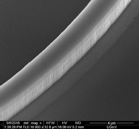
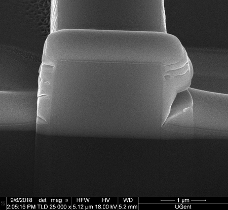
The result of the interaction between the plasma and the material is very sensitive to the different parameters (sample size, pressure, gas concentration, potential…). Thus, optimization of these parameters is required in order to obtain straight and smooth waveguide sidewalls. The waveguide loss increases with the roughness of the sidewalls.
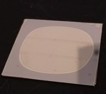
 Loading of samples in the chamber of a RIE system. |
 Etching of 2um Ge-on-Si structures. In the edges of the samples |
 SEM micrograph showing the sidewalls on a waveguide bend. |
 SEM micrograph of a FIB section showing the profile of a waveguide. |
In addition to the etching process, in the reaction chamber other physical (e.g. heating) and chemical (e.g. recombination) processes with occur, leading to different effects and by-products. In our case we use a combination of SF6, CH4 and H2 to etch the germanium. One potential side effect of the etching process is the formation and deposition of fluorinated polymers on the sample.
Those polymers could potentially lead not only to an increase of propagation loss but also modify surface properties (hydrophobicity) of the fabricated waveguides which ultimately would result in compatibility issues with the deposition of a coating.
After fabrication, samples are examined under SEM (Scanning electron microscope) in order to verify their quality. In addition, XPS (X-ray photoelectron spectroscopy) analysis can be used to screen for potentially deposited by-products.
The etch depth is controlled by the etching time. Depending on the waveguide structure type, variations in depth will result in small or greater differences in behavior. For example, a variation of 100nm for a waveguide structure is negligible while for the current designs of gratings it will imply a reduction of efficiency by about 15-20%.

